Products
Epoxy molding compounds
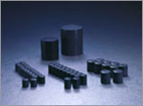
Encapsulation materials are packaging materials that protect semiconductor chips from heat, moisture, dust and physical impacts. While responding to diversifying semiconductor packaging and environmental issues, we offer products that meet our customers' requirements.
Anisotropic conductive films
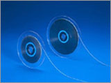
Hitachi Chemical was the first company in the world to develop these circuit connecting materials for displays. They satisfy both conductivity and insulation performance owing to adhesives with conductive particles, enable the connection of numerous minute electrodes at a time, and are used widely in devices such as PCs, cell phones, LCDs, and plasma TVs.
High-Tg glass epoxy copper-clad laminates for multilayer PWBs

These materials are made by impregnating glass cloth with epoxy resin and then laminating copper foil on both sides, and are used in multilayer printed wiring boards. The high-Tg glass epoxy copper-clad laminates maintain excellent FR-4 characteristics and at the same time realize high heat resistance and low moisture-absorption
Photosensitive Dry Films for Printed Wiring Board
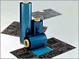
This is a film type resist that is which applied onto the copper-clad laminate to create circuits for the printed wiring boards. This features high sensitivity, high resolution, and high adhesion with strong tenting ability to create high density patterns.
CMP Slurry
CMP Slurry is a polishing material used in the chemical mechanical planarization (CMP) process to polish and smooth out the unevenness of the interlayer dielectric and in metal lines formed in the process of characterization. In addition to ceria-type slurry that minimize polishing damage and achieves excellent planarization properties for shallow trench isolation (STI), we also offer a lineup of the most advanced slurry for copper wiring formation.
Dicing Die bonding Film FH Series
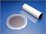
FH series is a two-in-one film with the functions for both dicing tape and die bonding film. Enabling both tapes to be laminated to a wafer at a time, it achieves easy handling of thinner wafer.

